Features of my latest DAC design:
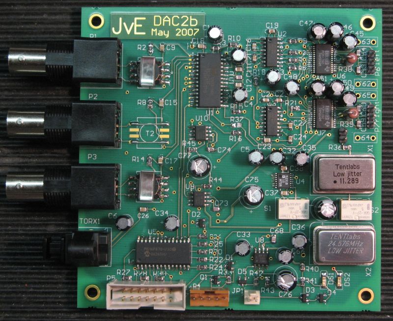
The main chips used for implementing the DAC are the Crystal CS8416 input receiver, a pair of TI PCM1792 audio dacs, and a PIC16F873 controller. The PCM1792 are each operated in 'mono' mode. Not only should this give a tiny more precise conversion, it gives in particular a double output current, which helps in obtaining enough 'drive' for my passive output. A pair of VCXOs (11.28MHZ and 24.57MHz) from tentlabs is used to natively operate on the input sample rate: sample rate conversion through digital filtering was considered undesired for accurate audio reconstruction.
To obtain a clean DAC clock, the VCXO input is driven from a small serial dac, controlled by a software PLL function in the PIC. This scheme inhibits any analog transfer of residuals from a dirty spdif inpuit clock to the PCM1738 audio dac chips. The quality of the clock is further improved by operating the CS8416 in ´slave´ mode, and by ´reclock´ buffers between the CS8416 and the PCM1738.
The analog audio output is (for now) truly passive, using a transformer coupling from the differential current output of the PCM1792 to a (single or symmetric) audio output voltage. Lundahl LL1674 are used for this purpose. They perform very well, but I still regard them as too expensive relative to the other DAC components. For the (near) future I intend to look into an active output stage.
A 10x10 cm2 PCB was designed with 4 metal layers to maintain a good ground plane. All digital logic is implemented with SMD components on the top side of the PCB. Note the application of small series-resistors in series with most of the digital lines, which helps to suppress interference, and which helps to keep a 'clean' (EMI-free) system. At the left side you see little HF transformers that decouple the SPDIF coax inputs.
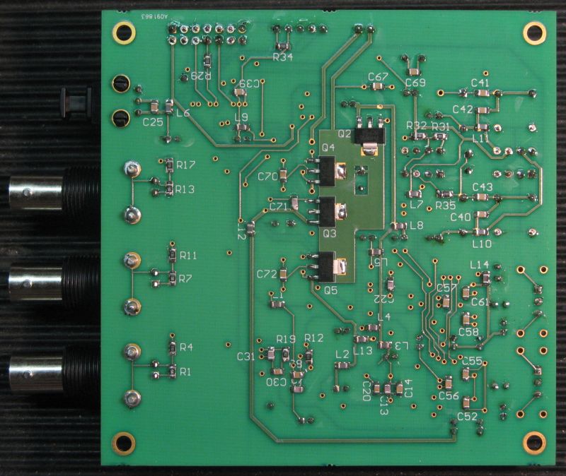
The PCB bottom side carries most analog components to create 5 separate low-noise power supplies,
with in particular separate power supplies for the left- and right-channel DAC chips.
The power supplies are stabilized with (green) LEDs as reference and
low-noise OPA2227 opamps for active regulation.
All digital ICs have individual capacitor powersupply decoupling,
and current feed through individual inductors for high-frequency damping.
By browsing the net, it seems hard to find examples on how to implement a good PLL with a PIC microcontroller. Let me try to explain how I did so, and just discuss the global concept: your own PLL design would probably anyhow be somewhat different. Note that I do not intend to explain here how PLLs in general work: that is not quite easy, and beyond the scope of this page.
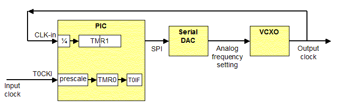
The goal of a clock recovery PLL is to create a high quality (read: very low jitter) clock signal from a lousy (noisy) input clock. 'Jitter' in a clock signal is the disturbance (error) in the supposedly uniform time period between successive (rising) edges of the clock signal. This 'jitter' has both an amplitude and a frequency aspect to it. To obtain good low-frequency jitter performance, the PLL as drawn above should adjust the VCXO clock frequency only slowly, and then only with small steps. Because we intend adjust the VCXO frequency only at low rate, the PIC has plenty of compute performance to implement a typical PLL low-pass filter.
The PIC operates itself on the clock of the VCXO. The 'dirty' input clock is routed to Timer0 in the PIC, which must be configured to run asynchronously. This Timer0 remains running, once enabled, and the firmware only reacts to the wrap-around moments, as flagged by the 'T0IF'.
The VCXO clock (the PIC internal clock) is passed to Timer1, which also continously keeps counting. The rate at which both counters do wrap-around is configured to be equal, by proper setting of the Timer0 prescaler. Every moment that T0IF gets set, the momentary value of Timer1 is captured. This is preferrably done as 'interrupt service routine', as it is important to have a constant (predictable) delay between the Timer0 wrap-around and the capturing of the Timer1 value. Note that neither counter is allowed to be stopped. If for example -as in my audio application- the VCXO runs at 11.289MHz (which is 256 x 44.1kHz, with 44.1kHz the digital audio sample rate), both counters wrap-around at approximately 43Hz (is 11.289MHz /4 /64K).
The captured value of Timer1 is a measure for the phase relation between both clock signals. (Or more accurate: for the phase relation between the divided-down 43Hz clocks). So at 43 Hz rate, the PIC computes the PLL low-pass filter on this 16-bit captured value, and sends the filtered result to the small serial-DAC to set the VCXO input.